Monday, April 26, 2021

Transistors: UNIZOR.COM - Physics4Teens - Electromagnetism - Semiconduct...

New lecture is released to UNIZOR.COM.
It's about transistors and the principles of using semiconductors in amplifying an analogue signal or working as ON/OFF switch.
UNIZOR.COM - Physics 4 Teens - Electromagnetism - Semiconductors in Electronics - Junction Transistors

Notes to a video lecture on http://www.unizor.com

Bipolar Junction Transistors

Below is a schematic representation of a so-called n-p-n bipolar junction transistor - one of the most popular types.

Functionally, it's playing a role similar to triodes discussed in one of the previous lectures. It can amplify a signal and it can work as On/Off switch.

To understand how it works, we will "build" it, step by step, gradually introducing new components.

As the first step in this process, imagine the device above without a narrow layer of p-type semiconductor in the middle and wiring connecting it to a battery (that is, without components marked in blue color).

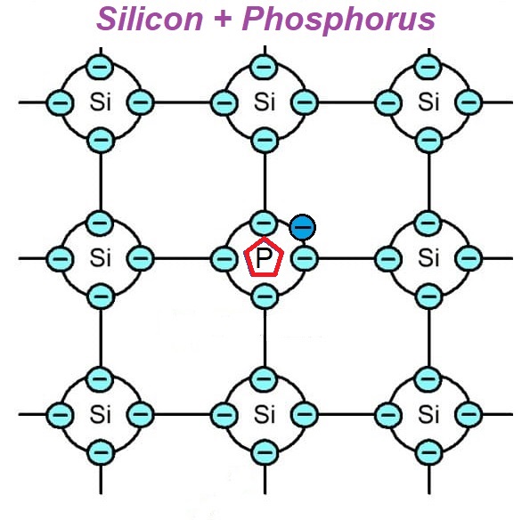
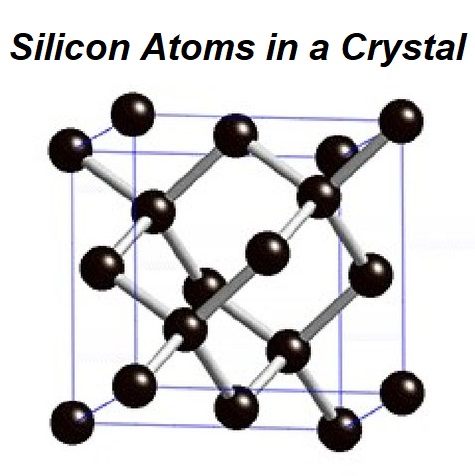
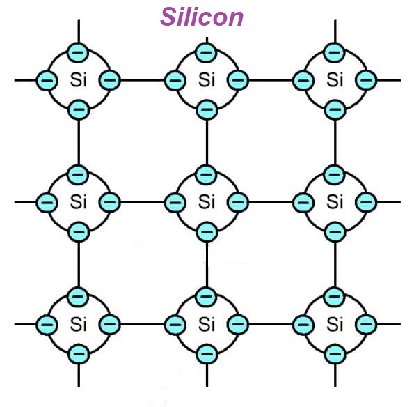
Then this device would represent a solid n-type semiconductor built, let's assume, from silicon foundation with added atoms of phosphorus that have excess of one valence electron for each atom, which does not fit into a crystalline structure of silicon.

This n-type semiconductor is attached to a battery through two electrodes.
Let's assume that the difference in electric potential (voltage) between electrodes is sufficient to attract extra valence electrons of phosphorus (held only by electrostatic attraction to a nucleus, but not participating in covalent bonds) toward a positive electrode, but it's not strong enough to rip off other valence electrons participating in both the covalent bonds and electrostatic attraction to a nucleus, as electrons of silicon atoms are.

When such voltage is present between the electrodes, there is a small current going through a semiconductor, as the extra valence electrons from phosphorus atoms will be attracted to a positive electrode, rendering these phosphorus atoms positively charged, while the negative electrode will compensate the loss of electrons in the body of a semiconductor.
The current, obviously, depends on density of phosphorus atoms within silicon foundation and voltage applied.

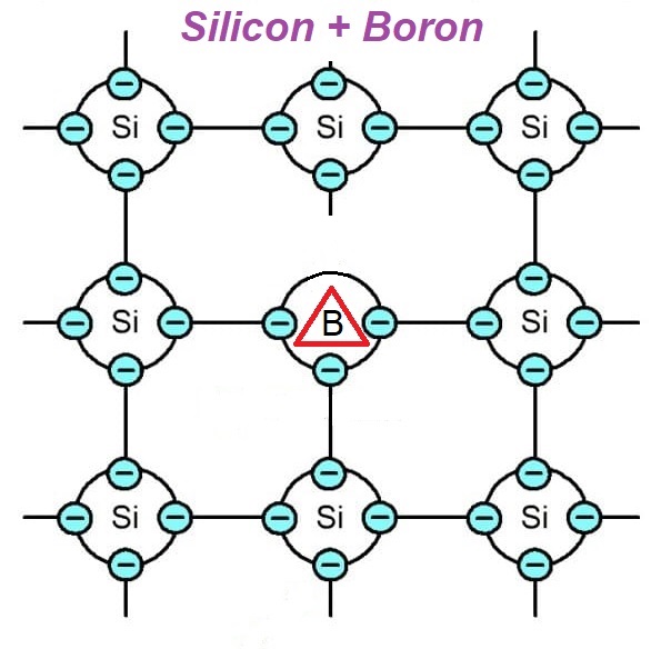
The next step is to split the solid n-type semiconductor in two halves and put a layer of p-type semiconductor (let's assume its silicon with boron additive) in between two halves of n-type semiconductor (thin blue layer on the picture above represents this p-type semiconductor). Let's not connected this p-type semiconductor to a battery yet.

This will stop the current and here is why.
As before, the positive electrode will attract extra valence electrons of phosphorus atoms from the n-type semiconductor (the right side on the picture above).

The other side of n-type semiconductor, connected to a negative electrode, will have its extra valence electrons of phosphorus penetrating the n-p junction into p-type semiconductor. Both random moving of these free electrons and repelling off the negative electrode are the factors in this process. Crossed the n-p junction, they will be captured by holes in the covalent bonds of p-type semiconductor.

After some time there will be a saturation of the covalent bonds in the p-type semiconductor and the flow of electrons from the n-type to p-type stops, as the barrier of extra electrons in the p-type layer would repel electrons from the n-type connected to a negative electrode.

At this time the covalent bonds of the p-type layer will be filled, which renders it to be negatively charged. Extra electrons around boron nuclei will be held only by covalent bonds, but not attracted to a nucleus.
The n-type connected to a negative electrode will be neutral, as the electrons crossed to the p-type layer through n-p junction will be compensated from the negative electrode.
The n-type connected to a positive electrode will be positively charged, as its free valence electrons, not participating in covalent bonds, will be consumed by a positive electrode.

Now we will introduce the last component of this device - connect the p-type layer to a positive electrode of another battery and the negative electrode of this battery connect to the n-type semiconductor that already has a connection to a negative electrode of another battery.
Thus this n-type semiconductor will be connected to negative electrodes of both batteries.

What's important now is that the electrons, crossed into p-type layer through n-p junction, making it negatively charged and making a barrier on the migration of new electrons from the n-type semiconductor connected to a negative electrode, will be attracted by a positive electrode of a new battery. These electrons are held only by covalent bonds inside the p-type layer, not the electrostatic attraction to a nucleus. Positive electrode of a new battery will attract some of them from the place where they acted as a barrier at the n-p junction, the barrier weakens, and new electrons from the n-type semiconductor could penetrate the n-p junction barrier into p-type layer.

The process does not stop here. Since the barrier is weakened, the electrons from n-type semiconductor connected to a negative electrode continue migrating to p-type layer. That's why this n-type semiconductor is called emitter. Some of these electrons go further through p-n junction between a p-type layer and the other n-type semiconductor connected to a positive electrode, establishing an electric current between two initial electrodes. That's why that other n-type semiconductor is called collector. The semiconductor of p-type, making the layer between emitter and collector is called base.

By changing the voltages on two batteries involved and by changing the amounts of additives into emitter, collector and base we can control the current between emitter and collector.

Under some conditions the n-p-n bipolar junction transistor, whose principles of work are described above, can act as an amplifier of the signal between emitter and base into a stronger signal between emitter and collector.

Under some other conditions n-p-n bipolar junction transistor can act as the On/Off switch, opening or closing a circuit between emitter and collector by applying some voltage between emitter and base.

There are other ways to connect emitter, collector, base and batteries that we will not consider, as our purpose is to introduce a concept, rather than going into details of implementation. The development of contemporary transistors, their theoretical and technological aspects took a lot of efforts and time, so now we have a pretty advanced devices. But the principles of their work are still the same, those we demonstrated on the example presented above.

Thursday, April 22, 2021

p-n Junction Diodes: UNIZOR.COM - Physics4Teens - Electromagnetism - Sem...

Notes to a video lecture on http://www.unizor.com

p-n Junction Diodes

Consider a semiconductor of n-type, like silicon (Si) with phosphorus (P) additive.
Atoms of P with its five valence electrons are embedded in the crystalline structure of Si with four of these valence electrons falling nicely into a structure, making covalent bonds with four neighboring atoms of Si, while the fifth one cannot get a pair to establish a covalent bond, so it's rather loosely attached to its atom of P and might randomly travel around.


During this process of randomly fluctuating electrons within an n-type of a semiconductor the whole structure remains electrically neutral because these traveling negatively charged electrons are balanced by extra protons in atoms of phosphorus.

The number of these traveling electrons is not great, so, if we apply a low voltage to a semiconductor, we can observe some low conductivity, but increasing the voltage will show that the conductivity is greater. The mechanism of this conductivity is based on a combination of electrostatic forces and forces of covalent bonds that maintain a crystalline structure of a semiconductor.

Freely traveling excess electrons of an n-type semiconductor will be electrostatically attracted by a positive electrode that has deficiency of electrons. Then the body of a previously electrically neutral semiconductor becomes positively charged, since it lost some electrons. Consequently, electrons from a negative electrode will enter the semiconductor, will not be captured by covalent bonds and become free traveling ones, replacing those consumed by a positive electrode.

This process of electrons moving from a negative electrode through an n-type semiconductor to a positive electrode will continue, as long as the voltage between electrodes is maintained at sufficient level.

Now consider a p-type semiconductor, like silicon (Si) with boron (B) additive.
Atoms of B, embedded in the crystalline structure of Si, have their three valence electrons bonded to valence electrons of three surrounding atoms of Si, while one valence electron of the fourth neighboring atom of Si cannot get a pair to establish a covalent bond with atom of B, thus a hole in the crystalline structure is formed.

Any neighboring atom of Si, if properly excited, can have its valence electron to jump from its own atom to fill the gap. That leaves a hole in another spot of a crystalline structure. Then some other electron from yet another atom can fill the new hole, opening a hole in yet another area. So, holes in the crystalline structure are randomly traveling inside a p-type of semiconductor.

This process of randomly moving holes in the crystalline structure of p-type semiconductor is analogous to the above described random moving of electrons in the n-type semiconductor.

It also assures that, if a sufficient voltage is applied to this type of semiconductor, the conductivity can be observed. The mechanism of this conductivity is based on a combination of electrostatic forces and forces of covalent bonds that maintain a crystalline structure of a semiconductor.

Consider holes in the crystalline structure caused by a deficiency of one valence electron of atoms of B. There are electrons randomly traveling from a negative electrode into a semiconductor and back. Some electrons that happened to be in the vicinity of a hole will be captured by the forces of covalent bonds and fill the holes in the crystalline structure.
Then the semiconductor will become negatively charged, that is will have excess of electrons. The excess electrons will be attracted by a positive electrode and new holes will be created in the crystalline structure.

This process of electrons moving from a negative electrode through a p-type semiconductor to a positive electrode and, correspondingly, holes moving in the opposite direction will continue, as long as the voltage between electrodes is maintained at sufficient level.

Next topic is to analyze the behavior of electrons and holes at the border or junction between the n-type semiconductor and the p-type one. This border area is called p-n junction.

Initially electrically neutral, a semiconductor on the n-type side of a junction has electrons that do not fit in its crystalline structure and not involved in the covalent bonding.
On the p-type side of a junction, also initially electrically neutral, there are holes in the crystalline structure of a semiconductor waiting to capture some electron into a covalent bonding.

The first consideration is related to activity related to the forces of covalent bonds. Randomly traveling electrons from the n-type semiconductor can jump through a junction into the p-type semiconductor and be captured by covalent bonds to restore missing electrons of a crystalline structure of a semiconductor in the area adjacent to the junction.

That, in turn, creates a layer of negative charge near the junction on the p-type side and a positively charged layer near the junction on the n-type side.

Excess electrons kept by covalent bonds near the junction on the p-type side act as an electrostatic barrier to prevent new electrons from the n-type side to jump the junction.
Some kind of equilibrium is developed between electrons on the n-type side not involved in the crystalline structure and ready to jump the junction and electrons already jumped to the p-type side.

The covalent bonds are restored on the p-type side and there are no electrons not linked through covalent bonds on the n-type side of the junction. The price for this proper crystalline structure on both sides of a junction is that there is an excess electrons on the p-type side and deficiency of electrons on the n-type side.

Let's connect the p-type side of a junction to a positive electrode and the n-type to a negative electrode of a battery.
Excess electrons from the p-type will be attracted to a positive electrode and the barrier of electrons on the p-type side that prevented new electrons from the n-type to jump the junction will no longer be there.

This will cause new electrons from the n-type side to be able to jump the junction into p-type. In parallel, electrons from the negative electrode will be attracted to a positively charged n-type side, compensating electrons that have already jumped to the p-type side.

As we see, there will be an electric current through a p-n junction, as long as the voltage is maintained.

Now let's connect the electrodes in an opposite way. Positive to n-type side and negative to the p-type.
Electrons that do not fit a crystalline structure on the n-type will be attracted to a positive electrode and will no longer participate in the process.
New electrons from the negative electrode will penetrate the body of the p-type side filling all the covalent bonds and reinforcing the electrons' barrier near a junction to completely stop all flow of electrons from the n-type side.

Now the crystalline structure on both sides of a p-n junction are complete and no new electrons are traveling in any direction. There is no current through a p-n junction.

As we see, the electrons can go through a p-n junction only if n-type side is connected to a negative electrode and p-type side is connected to a positive electrode. So, p-n junction acts like a diode. This configuration of p-type and n-type semiconductors joined together and acting as a diode is called p-n junction diode.

Saturday, April 17, 2021

Covalent Bonds: UNIZOR.COM - Physics4Teens - Electromagnetism - Theory o...

Notes to a video lecture on http://www.unizor.com

Covalent Bonds

Now we know that the theory of semiconductors is built upon introducing some impurity into crystalline structure of such a material as silicon (Si) or germanium (Ge).
Let's consider this crystalline structure in more details to understand its underlying principles.

According to the orbital model of an atom, electrons are rotating around a nucleus on certain orbits, each orbit representing certain energy level possessed by all electrons on it. There are certain principles related to quantum mechanics and wave theory of elementary particles that prescribe electrons to rotate only on certain distinct radiuses around a nucleus. The reason for this we will discuss when addressing the atomic structure in more details in a corresponding part of this course.

On every distinct radius the rotating electrons experience the attraction of the protons in a nucleus and repelling of other electrons rotating on the same orbit (on the same radius from a nucleus). Obviously, for every distinct radius of an orbit there is a maximum number of electrons that can rotate around a nucleus without pushing each other so strongly that one of them must jump out of the orbit to, most likely, the orbit of a larger radius or even outside of the atom.

Calculations based on principles of quantum mechanics show that this maximum number for the first (closest to a nucleus) orbit is 2, for the next - 8, next - 18 etc. The formula N=2n² where n is the orbit number and N is the maximum number of electrons on this orbit describes this in many (but not all) cases.

The atom of every element has certain number of protons in a nucleus and the same number of electrons rotating on different orbits. These orbits are packed with electrons not to exceed their maximum capacity.

In a simplified model of an atom of carbon C12 with 6 protons and 6 neutrons in a nucleus there are 6 electrons on two orbits: 2 on the closest to a nucleus and 4 on the next one.


In a simplified model of an atom of silicon Si28 with 14 protons and 14 neutrons in a nucleus there are 14 electrons on three orbits: 2 on the closest to a nucleus, 8 on the next one and 4 on the outer most orbit.


In a simplified model of an atom of titanium Ti48 with 22 protons and 26 neutrons in a nucleus there are 22 electrons on four orbits with, correspondingly, 2, 8, 10 and 2 electrons on them.


In a simplified model of an atom of radon Rn222 with 86 protons and 136 neutrons in a nucleus there are 86 electrons on five orbits with, correspondingly, 2, 8, 18, 32, 18 and 8 electrons on them.


Electrons populating the outer most orbit are called valence electrons. While in theory belonging to particular atoms, they are very active in their relationships with other atoms and their valence electrons.

In fact, valence electrons from different atoms might bond together, thus two atoms have a shared pair of electrons. The reason to this is a tendency to fill up the orbit of valence electrons. The magic number of valence electrons is 2 for atoms with only one orbit (there are only two elements with a single orbit of electrons - hydrogen and helium) or 8 for atoms with two or more orbits, so two or more atoms might come into bonding by sharing the valence electrons, thus filling all outer orbits up to a magic number of electrons (shared and not shared).

Here is an example of a molecule of methane that consists of one atom of carbon C12 (two orbits with 2 electrons on an inner orbit, not shown on a picture, and 4 valence electrons) and four atoms of hydrogen H1 (single orbit with 1 electron on it).

As we see, the orbit with valence electrons of an atom of carbon has now 8 electrons, 4 its own and 4 shared with atoms of hydrogen, thus filling a magic number of valence electrons. At the same time each atom of hydrogen has 2 electrons (also a magic number for an atom of hydrogen), 1 its own and one shared with an atom of carbon.

These covalent bonds between atoms are the basis for certain different atoms to combine into molecules or the same atoms to form a crystalline structure.

Consider now a crystalline structure of a silicon, our main subject of discussion.
Each atom of silicon contains 4 valence electrons on its outer (third) orbit. In three-dimensional world these electrons are positioned at the vertices of a tetrahedron with a nucleus of an atom at the center of this tetrahedron.
Four valence electrons of one atom of silicon pair with valence electrons of neighboring atoms to form a complicated three-dimensional crystalline structure that in two-dimensional representation looks as follows.

Four neighboring silicon atoms contribute to a center one their valence electrons to share (one from each neighbor), thus the center atom has a magic number of electrons on its outer orbit. Each valence electron of each atom is shared with a neighboring atom and, therefore, every atom has 8 electrons (including both its own 4 electrons and 4 from its four neighbors, one from each). This makes a strong crystalline structure of material.


Thursday, April 8, 2021

Theory of Semiconductors: UNIZOR.COM - Physics4Teens - Electromagnetism ...

Notes to a video lecture on http://www.unizor.com

Theory of Semiconductors

Conductivity is the quality of a material to conduct electricity. Since electricity is carried by electrons, it's important how "free" electrons are in the material and how easy it is for negatively charged electrons to fly away from attraction of a positively charged nucleus of an atom.

Electrons can circle around a nucleus on certain stationary orbits (more precisely, narrow bands of orbits). So, to fly away from a nucleus, electron needs certain amount of energy to jump over a gap from one orbit to a higher one and, eventually, to fly away. If the distance between bands of an atom is minimal, electrons will jump over the gap between them easier and, potentially, the conductivity of this type of a material is better. If this gap is large, conductivity will be lower or none at all.

It happens that most metals have a very small gap between the bands of electron orbits, so electrons can relatively free jump from one band to a higher one and, eventually, fly away from their nuclei to other nuclei, thus making enough free electrons to facilitate the electric current. That's why metals are good conductors of electricity.

On another hand, diamonds have atoms with large gap between the bands of electron orbits, which makes it very difficult for electrons to escape the attraction of their nuclei. It's not impossible, but needs a lot of energy to excite them, enabling a long jump from one band to the next. This makes diamond and other elements with large gap between the bands insulators.

Finally, there is an "in-between" kind of elements with gaps between bands of electron orbits larger than in metals, but still not large enough, so relatively small energy supplied to electrons (heat, light etc.) will make them conductors, while without this extra energy they are insulators. These elements are semiconductors.

Let's start with the most important example of a semiconductor - silicon (Si).
Silicon is a metalloid, it has crystalline structure and its atoms have four valence electrons on the outer most orbit, next down orbit contains eight electrons and the inner most - two electrons.

Silicon is one of the most frequently occurring elements on Earth and, together with oxygen, forms molecules of silicon dioxide SiO2 - main component of sand.

All silicon atoms are neutral since the number of electrons in each one and the number of protons in each nucleus are the same and equal to 14.
Atoms are connected by their covalent bonds of valence electrons on the outer orbits into a lattice-like crystalline structure.

Picture below represents the crystalline structure of silicon

For the purposes of this lecture we will represent inner structure of silicon atoms with only outer orbit of each atom with four valence electrons, as electrons on the inner orbits do not participate in the process of generating electricity from light.

The covalent bonds are quite strong, they do not easily release electrons. As a result, under normal conditions silicon is practically a dielectric.
However, if we excite the electrons sufficiently enough to break the covalent bonds, some electrons will move. For example, if we increase the temperature of a piece of silicon or put it under a bright sun light and measure its electrical resistance, we will observe the resistance diminishing.
That's why silicon and similar elements are called semiconductors.

While excited electrons of any semiconductor decrease its electrical resistance, they don't produce electromotive force because the material as a whole remains electrically neutral.
To build a semiconductor that conducts electricity we will introduce two kinds of "impurities" into crystalline lattice of silicon.
One is an element with five valence electrons on the outer most orbit, like phosphorus (P). When it's embedded into a crystalline lattice of silicon, one electron on that outer orbit of phosphorus would remain not attached to any neighboring atom through a covalent bond.

This creates the possibility for this electron to start traveling, replacing other electrons and pushing them out, which are, in turn, push out others etc. Basically, we create as many freelance electrons as many atoms of phosphorus we add to silicon base.
The whole material is still neutral, but it has certain number of freelance electrons and the same number of stationary positive ions - those nuclei of phosphorus that lost electrons to freelancers.
Silicon with such addition is called n-type (letter n for negative).

Another type of "impurity" that we will add to silicon is an element with three valence electrons on the outer orbit, like boron (B).
When atoms of boron are embedded into a crystalline lattice of silicon, the overall structure of this combination looks like this

In this case the lattice has a deficiency of an electron that is traditionally called a "hole". Existence of a "hole" opens the opportunity for neighboring valence electrons to fill it, thus creating a "hole" in another spot. These "holes" behave like positively charged particles traveling inside silicon with added boron inasmuch as negatively charged electrons travel in silicon with added phosphorus.
Silicon with such addition of boron is called p-type (letter p for positive).

Now imagine two types of "impure" silicon, n-type and p-type, contacting each other. In practice, it's two flat pieces (like very thin squares) on top of each other.
Let's examine what happens in a thin layer of border between these different types of material.

Initially, both pieces of material are electrically neutral with n-type having free traveling electrons and equal number of stationary positive nuclei of phosphorus inside a crystalline structure and with p-type having traveling "holes" and equal number of stationary positive nuclei of boron inside a crystalline structure.

As soon as contact between these two types of material is established, certain exchange between electrons of the n-type material and "holes" of the p-type takes place in the border region called p-n junction. Electrons and "holes" in this border region combine, thus reconstituting the lattice.
This process is called recombination.

The consequence of this process of recombination is that n-type material near the border loses electrons, thus becoming positively charged, while the p-type gains the electrons, that is loses "holes", thus becoming negatively charged.

Eventually, the diffusion between n-type and p-type materials stops because negative charge of the p-type sufficiently repels electrons from the n-type. There will be some equilibrium between both parts.

These qualities of n-type and p-type semiconductors, as well as the processes occurring in a thin layer between these two types of semiconductors allow to use them in electronics. Transistors are electronic devices made of semiconductors and functionally equivalent to electronic devices described in the previous section and made using vacuum tubes.
The details of usage semiconductors in electronics will be presented in the next lectures.