Theory of Semiconductors
Conductivity is the quality of a material to conduct electricity. Since electricity is carried by electrons, it's important how "free" electrons are in the material and how easy it is for negatively charged electrons to fly away from attraction of a positively charged nucleus of an atom.
Electrons can circle around a nucleus on certain stationary orbits (more precisely, narrow bands of orbits). So, to fly away from a nucleus, electron needs certain amount of energy to jump over a gap from one orbit to a higher one and, eventually, to fly away. If the distance between bands of an atom is minimal, electrons will jump over the gap between them easier and, potentially, the conductivity of this type of a material is better. If this gap is large, conductivity will be lower or none at all.
It happens that most metals have a very small gap between the bands of electron orbits, so electrons can relatively free jump from one band to a higher one and, eventually, fly away from their nuclei to other nuclei, thus making enough free electrons to facilitate the electric current. That's why metals are good conductors of electricity.
On another hand, diamonds have atoms with large gap between the bands of electron orbits, which makes it very difficult for electrons to escape the attraction of their nuclei. It's not impossible, but needs a lot of energy to excite them, enabling a long jump from one band to the next. This makes diamond and other elements with large gap between the bands insulators.
Finally, there is an "in-between" kind of elements with gaps between bands of electron orbits larger than in metals, but still not large enough, so relatively small energy supplied to electrons (heat, light etc.) will make them conductors, while without this extra energy they are insulators. These elements are semiconductors.
Let's start with the most important example of a semiconductor - silicon (Si).
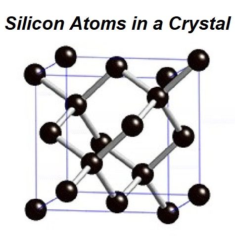
Silicon is a metalloid, it has crystalline structure and its atoms have four valence electrons on the outer most orbit, next down orbit contains eight electrons and the inner most - two electrons.
Silicon is one of the most frequently occurring elements on Earth and, together with oxygen, forms molecules of silicon dioxide SiO2 - main component of sand.
All silicon atoms are neutral since the number of electrons in each one and the number of protons in each nucleus are the same and equal to 14.
Atoms are connected by their covalent bonds of valence electrons on the outer orbits into a lattice-like crystalline structure.
Picture below represents the crystalline structure of silicon
For the purposes of this lecture we will represent inner structure of silicon atoms with only outer orbit of each atom with four valence electrons, as electrons on the inner orbits do not participate in the process of generating electricity from light.
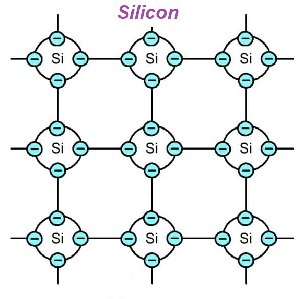
The covalent bonds are quite strong, they do not easily release electrons. As a result, under normal conditions silicon is practically a dielectric.
However, if we excite the electrons sufficiently enough to break the covalent bonds, some electrons will move. For example, if we increase the temperature of a piece of silicon or put it under a bright sun light and measure its electrical resistance, we will observe the resistance diminishing.
That's why silicon and similar elements are called semiconductors.
While excited electrons of any semiconductor decrease its electrical resistance, they don't produce electromotive force because the material as a whole remains electrically neutral.
To build a semiconductor that conducts electricity we will introduce two kinds of "impurities" into crystalline lattice of silicon.
One is an element with five valence electrons on the outer most orbit, like phosphorus (P). When it's embedded into a crystalline lattice of silicon, one electron on that outer orbit of phosphorus would remain not attached to any neighboring atom through a covalent bond.
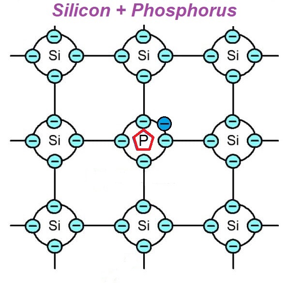
This creates the possibility for this electron to start traveling, replacing other electrons and pushing them out, which are, in turn, push out others etc. Basically, we create as many freelance electrons as many atoms of phosphorus we add to silicon base.
The whole material is still neutral, but it has certain number of freelance electrons and the same number of stationary positive ions - those nuclei of phosphorus that lost electrons to freelancers.
Silicon with such addition is called n-type (letter n for negative).
Another type of "impurity" that we will add to silicon is an element with three valence electrons on the outer orbit, like boron (B).
When atoms of boron are embedded into a crystalline lattice of silicon, the overall structure of this combination looks like this
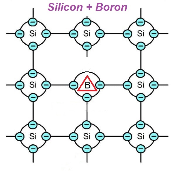
In this case the lattice has a deficiency of an electron that is traditionally called a "hole". Existence of a "hole" opens the opportunity for neighboring valence electrons to fill it, thus creating a "hole" in another spot. These "holes" behave like positively charged particles traveling inside silicon with added boron inasmuch as negatively charged electrons travel in silicon with added phosphorus.
Silicon with such addition of boron is called p-type (letter p for positive).
Now imagine two types of "impure" silicon, n-type and p-type, contacting each other. In practice, it's two flat pieces (like very thin squares) on top of each other.
Let's examine what happens in a thin layer of border between these different types of material.
Initially, both pieces of material are electrically neutral with n-type having free traveling electrons and equal number of stationary positive nuclei of phosphorus inside a crystalline structure and with p-type having traveling "holes" and equal number of stationary positive nuclei of boron inside a crystalline structure.
As soon as contact between these two types of material is established, certain exchange between electrons of the n-type material and "holes" of the p-type takes place in the border region called p-n junction. Electrons and "holes" in this border region combine, thus reconstituting the lattice.
This process is called recombination.
The consequence of this process of recombination is that n-type material near the border loses electrons, thus becoming positively charged, while the p-type gains the electrons, that is loses "holes", thus becoming negatively charged.
Eventually, the diffusion between n-type and p-type materials stops because negative charge of the p-type sufficiently repels electrons from the n-type. There will be some equilibrium between both parts.
These qualities of n-type and p-type semiconductors, as well as the processes occurring in a thin layer between these two types of semiconductors allow to use them in electronics. Transistors are electronic devices made of semiconductors and functionally equivalent to electronic devices described in the previous section and made using vacuum tubes.
The details of usage semiconductors in electronics will be presented in the next lectures.

No comments:
Post a Comment