Implementation of Electronic
Flip Flop (Latch)
In the beginning of computer era one of the first problem was to be able to store information. And the first step was to design a circuit that can store one bit of information, 1 or 0.
A digital flip-flop or latch is such a one bit storage, an electronic device that
(a) has two states (1 and 0);
(b) can be set to one of these two states by a proper impulse;
(c) retains the state after an impulse is gone.
The main component of a design we will discuss in this lecture is a combination of a binary logical operation OR and a unary logical operation NOT, both of which were discussed in previous lectures.
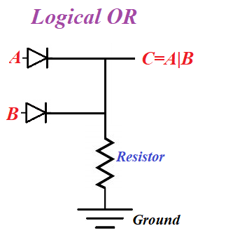
Let's recall the implementation of the logical OR circuit that involves diodes.
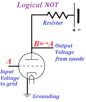
The implementation of the NOT logical operation that involves triodes was suggested as follows
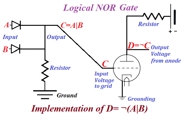
Combining them sequentially, we first implement OR and then NOT of the result of OR, thus implementing the binary logical operation NOR as follows
NOT(A OR B) = ¬(A|B)
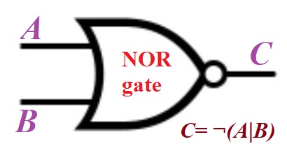
The logical NOR operation is denoted by the following symbol
The table below denotes the results of NOR operation for all pairs of input values of arguments
¬(0|0) = ¬0 = 1
¬(0|1) = ¬1 = 0
¬(1|0) = ¬1 = 0
¬(1|1) = ¬1 = 0
Using the NOR gate, we will implement a circuit that can serve as a one bit memory cell.
Consider the following schema of a circuit called SR flip-flop or SR latch.
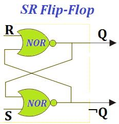
Here terminals R (Reset) and S (Set) are controlling terminals, using which we store information.
Information is stored in a pair of terminals Q and its opposite NOT(Q)=¬Q in a way that either Q=1 (and ¬Q=0) or Q=0 (and ¬Q=1).
These two states are stable in a sense that, after we send a positive impulse at terminal S, while R=0, the Q will be equal to 1 irrespective of its prior value, the ¬Q will be equal to 0 irrespective of its prior value, and they both will retain the same values Q=1 and ¬Q=0 after the impulse at S is gone (that is when S=0).
Similarly, after we send a positive impulse at terminal R, while S=0, the Q will be equal to 0 irrespective of its prior value, the ¬Q will be equal to 1 irrespective of its prior value, and they both will retain the same values Q=0 and ¬Q=1 after the impulse at R is gone (that is when R=0).
Let's examine the work of this SR latch in detail.
Set Q=1 and ¬Q=0
Assume, we set the voltage at terminal S to a positive value, keeping terminal R at zero potential. It means in logical sense that S=1 and R=0.
The NOR gate connected to terminal S, irrespective of its second connection to it, will produce a signal 0 as an output. Indeed, the OR operation between S=1 and any other signal produces 1 and NOT(1)=0.
This immediately sets ¬Q=0 and send zero potential to the NOR gate connected to terminal R that has zero potential. So, both inputs to NOR gate connected to R terminal are at zero potential. The logical OR of two zeroes is zero. Subsequent NOT converts the signal to 1 that sets terminal Q=1.
So, raising the potential at terminal S to a positive value, keeping terminal R at zero potential switches terminals Q and ¬Q to, correspondingly, values 1 and 0.
Let's see what happens when the positive impulse at terminal S is gone, so S=0, while terminal R is still at zero potential, terminal Q=1 and ¬Q=0.
The NOR gate connected to terminal S has one input from terminal S=0, while the other input is from terminal Q that was set to 1 on a previous step. The output from this NOR gate will be zero, since the logical OR between 0 and 1 gives 1, and subsequent logical NOT converts it to 0.
This sets ¬Q=0, but this terminal already had this value, so ¬Q does not change and remains at 0.
From there the value ¬Q=0 goes to the input of the NOR gate connected to terminal R that still has zero potential. Both input to this NOR gate are zero, so the output is 1, which sets Q=1, which it already has. So Q does not change and remains at 1.
As we see, the positive impulse on terminal S sets terminals Q and ¬Q to stable values 1 and 0 correspondingly, which they retain after the impulse is gone.
In other words, the positive impulse on terminal S sets a flip-flop to a stable state Q=1 and ¬Q=0.
Reset Q=0 and ¬Q=1
Notice how symmetrical is the circuit of our flip-flop.
Sending a positive impulse to terminal R, while keeping zero potential on terminal S is fully analogous to a previous case, except now the flip-flop will be in a stable state Q=0 and ¬Q=1.
Conclusion
The flip-flop presented above can serve as a memory bit, since we can set its value to 1 (Q=1 and ¬Q=0) by sending a positive impulse to terminal S or to 0 (Q=0 and ¬Q=1) by sending a positive impulse to terminal R.
An important detail about this design is that we should never have a situation when both S=1 and R=1. The reason is, the state of a flip-flop in this cases is unpredictable, it will constantly change the values on its output terminals. So, this situation of both input terminals being equal to 1 must be avoided.
Allowed are only positive impulse (that is, an electric potential jumps to some positive value, after which it goes down to zero) on terminal S, keeping R=0, which sets the value of a flip-flop to 1 (that is, Q=1 and ¬Q=0) or positive impulse on terminal R, keeping S=0, which sets the value of a flip-flop to 0 (that is, Q=0 and ¬Q=1).


No comments:
Post a Comment